Tuesday, 18 October 2011

Experiment 5 (99 Counter)

I. Introduction:

                In this experiment 5, our group used the QUARTUS II software package to design and simulate a 99 counter. Counters are finite state machines that go from one state to another on each clock pulse. With a general finite state machine the next state that the system goes to depends on the present state and the present inputs. With a counter the next state only depends on the present state. As an example consider a decade down counter. This counter will count through 00 to 99. Each clock pulse forces the counter to the next state or binary output pattern.
               
II. Objective:

To be able to create a 99 counter with previous symbols.

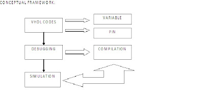
III. Conceptual Framework:


IV. Data and Results:

library ieee;
use ieee.std_logic_1164.all;
entity exp5 is 

port(
reset : in  BIT;
clk : in  BIT;
pause : in  BIT;
set : in  BIT;
o : OUT BIT;
int  : IN INTEGER RANGE 0 TO 9;
r : out bit_vector(3 downto 0);
a : out bit_vector(3 downto 0));

                                                                                   
end exp5;

architecture exp5 of exp5 is  


BEGIN

PROCESS (clk, reset, pause)
                                                                                   
VARIABLE temp : INTEGER RANGE 0 TO 10 := 0;                 
                                                                                               

BEGIN                                                                    
IF (clk'EVENT AND clk = '1') THEN               
if (pause = '0') THEN
temp := temp;
else                                                                        
temp := temp + 1;
                                                                                 
o <= '0';
end if;
IF (temp = 10) THEN                                        
temp := 0;                                                                          


else


END if;
END if;

Results:

DIAGRAM OF EXP 5


V. Analysis:
                  In this experiment, the counter circuit arrives at 99. We analyzed this circuit may on the same wave length certainly. It feed a signal clock at 14 pin cause the position logic at a pin output. From 0 to 99 for switch performs choose RUN or Reset. By seeing the data will understand increasingly.

VI. Conclusion:
                    Therefore, we concluded that we could derive the equation that describe this counter and implement the 99 counter in dataflow architecture in VHDL. Alternatively, we could describe the structure in terms of AND gates, OR gates, NOT gates and flip-flops. This would be a structural architecture in VHDL.



Experiment 4 (Sequential Code)

I. Introduction:

      In this experiment 4 our group used the QUARTUS II software package to design and simulate a sequential logic circuit. The requirements for this experiment consists of completing the QUARTUS II designs, printing VHDL source files and simulation results, and completing the laboratory report.   
          
        This hardware laboratory exercise is designed to introduce you to a modern computer aided design tool for hardware called Quartus II. The Quartus II software is available on the Windows machines in the laboratory.

       Implement the following circuits using VHDL. Provide a timing simulation for the DE2 board. Devise a set of test vectors to verify the circuit. The said experiment gives detailed information on how to create a sequential logic circuit with sequential code.

II. Objective:

To be able to create sequential logic circuit with sequential code.


III. Conceptual Framework


IV. DATA and RESULTS:

library ieee;
use ieee.std_logic_1164.all;


entity exp4 is 
port(reset : in  BIT;clk : in  BIT;
pause : in  BIT;
set : in  BIT;
o : OUT BIT;
 int  : IN INTEGER RANGE 0 TO 9;
r : out bit_vector(3 downto 0);
 a : out bit_vector(3 downto 0));
end exp4;

architecture exp41 of exp4 is  
BEGIN
 PROCESS (clk, reset, pause;
VARIABLE temp : INTEGER RANGE 0 TO 10 := 0; 
BEGIN                                                                    
IF (clk'EVENT AND clk = '1') THEN               
if (pause = '0') THEN
temp := temp;
else                                                                        
temp := temp + 1;
                                                                                 

end if;
IF (temp = 10) THEN                                        
temp := 0;                                                                                                                                                                                                                                                                                                                          
else                                                                                                                       
                                                                                                                                          
END IF;                                                                                
END IF;                                                                                
IF (reset = '0') THEN                                                       
temp := 0;                                                                                          
END IF;

CASE temp IS
                                                                                               
WHEN 0 => r <= "0000" ;
WHEN 1 => r <= "0001" ;                                
WHEN 2 => r <= "0010" ;                                
WHEN 3 => r <= "0011" ;                                
WHEN 4 => r <= "0100" ;                                
WHEN 5 => r <= "0101" ;                                
WHEN 6 => r <= "0110" ;                                
WHEN 7 => r <= "0111" ;                                
WHEN 8 => r <= "1000" ;
WHEN 9 => r <= "1001" ;                                
WHEN OTHERS => null;                                                 
END CASE;

CASE int IS
                                                                                               
WHEN 0 => a <= "0000" ;                                
WHEN 1 => a <= "0001" ;                                
WHEN 2 => a <= "0010" ;                                
WHEN 3 => a <= "0011" ;                                
WHEN 4 => a <= "0100" ;                                
WHEN 5 => a <= "0101" ;                                
WHEN 6 => a <= "0110" ;                                
WHEN 7 => a <= "0111" ;                                
WHEN 8 => a <= "1000" ;                                
WHEN 9 => a <= "1001" ;
WHEN OTHERS => null;                                                 
END CASE;
IF (set = '0') THEN
temp := int;
  END IF;
END PROCESS ;
END exp41;

DIAGRAM OF EXPERIMENT 4

V. Analysis:

                  We show in this experiment that multilevel logic synthesis is an effective optimization strategy when targeting designs to lookup table-based FPGAs. Our data gives sequential code for a variable logic function used to illustrate the benefits of multilevel synthesis. In this experiment we will create a new design project which represents the sequential code in our data. Create a sequential design file that comprises the code from our results, as displayed in our data.

VI. Conclusion:

                    Therefore, we concluded that having implemented the design in the DE2 board, perform a timing simulation to gain a feeling for the timing characteristics of the DE2 board. Once a project has been compiled for the target device, it can be downloaded into a chip by using Quartus II. The procedure for programming a chip is described in our lectures and basically Quartus II is a useful tool for creating sequential logic circuit with sequential codes.

Experiment 3 (Concurrent Code and Symbol Interfacing)

I. Introduction:

                In this experiment our group creates the modules of the comparator and the multiplexer. The multiplexer codes are insert to the modules of 9 mod9 is the combinational circuits the comparator become the single working module that the program will run on it. The combination of the comparator and multiplexer codes.

II. Objective:

                To be able to implement combinational logic circuits with concurrent codes and interface their symbols with each other.


III. Conceptual Framework:


IV. Data and Results:

Multiplexer 3.1

library ieee;
use ieee.std_logic_1164.all;
use ieee.std_logic_arith.all;

entity mnm31 is
port (S : bit;
A,B : in bit_vector (0 to 3);
X : out bit_vector(0 to 3));
end mnm31;

architecture mux_Threep1 of mnm31 is
begin
process (S)
begin
case S is
when '0' => X<= A;
when '1' => X<= B;
end case;
end process;
end mux_Threep1;


Multiplexer 3.2

library ieee;
use ieee.std_logic_1164.all;

entity mnm32 is
port (A,B : in bit_vector (3 downto 0);
O : out bit);
end entity;

architecture comp of mnm32 is
begin
process (A,B)
begin
if (A(3) = '1' AND B(3) = '0') then O <='1';
elsif (A(2) = '1' AND B(2) = '0') then O <='1';
elsif (A(1) = '1' AND B(1) = '0') then O <='1';
elsif (A(0) = '1' AND B(0) = '0') then O <='1';
else
O <= '0';
end if;
end process;
end comp;

Results: 
Combinational of Multiplexer


V. Analysis:
                Our groups analyze and discuss how the comparator and multiplexer combine and the output is how the module reacts in two different inputs.

VI. Conclusion:

                We learned that the comparator and multiplexer combine to each other and we understand  the flow of the data in the comparator in and out and last the group is easily get the output of the experiment easily.


Experiment 2 (VHDL Familiarization)

I. Introduction:

                First the group is so familiar to the seven segment in the first experiment next Is the VHDL codes the program that we will use in the next experiment we should familiarize ourselves to make our work so familiar and good in the program of VHDL. We should know the characteristics of VHDL Support of modular hierarchical design.  Separate interface and body specifications of design entities. Multiple body specifications sharing the same interface (different levels of abstraction, alternatives, and versions). Late binding of bodies to entities using configurations.  Parameterized behavioral, structural and mixed descriptions. VHDL Common Intermediate form for simplified CAD tool access.

II. Objective:

                To be able to implement logic circuit design in VHDL codes

III. Conceptual Framework:

DIAGRAM OF DECODER:


DIAGRAM OF MULTIPLEXER


IV. Data and Results

                DECODER

library IEEE;
use IEEE.STD_LOGIC_1164.ALL;
use IEEE.STD_LOGIC_ARITH.ALL;

entity dec is
port (
        bcd : in std_logic_vector(3 downto 0); 
        F : out std_logic_vector(6 downto 0) 
    );
end dec;

architecture DEC1 of dec is
begin
process (bcd)
begin
case  bcd is
when "0000" => F<="0000001";
when "0001" => F<="1001111";
when "0010" => F<="0010010";
when "0011" => F<="0000110";
when "0100" => F<="1001100";
when "0101" => F<="0100100";
when "0110" => F<="0100000";
when "0111" => F<="0001111";
when "1000" => F<="0000000";
when "1001" => F<="0000100";
when "1010" => F<="0001000";
when "1011" => F<="1100000";
when "1100" => F<="1110010";
when "1101" => F<="1000010";
when "1110" => F<="0010000";
when "1111" => F<="0111000";
end case;
end process;
end DEC1;

Multiplexer

use ieee.std_logic_1164.all;

entity Mux is
port (A,B : in bit_vector (3 downto 0);
O : out bit);
end entity;

architecture comp of Mux is
begin
process (A,B)
begin
if (A(3) = '1' AND B(3) = '0') then O <='1';
elsif (A(2) = '1' AND B(2) = '0') then O <='1';
elsif (A(1) = '1' AND B(1) = '0') then O <='1';
elsif (A(0) = '1' AND B(0) = '0') then O <='1';
else
O <= '0';
end if;
end process;
end comp;

Results:

   Like in the first experiment the DE board will set the output of 1 to 15 which A=10, B=11 , C=12, D=13, E=14 and F=15. Then next is the multiplexer the output of this is same in the first multiplexer. When you tap the switch the output is the same.

V. Analysis:
                We analyze and discuss about the meaning of the VHDL codes in this codes the we should program the codes of the decoder and multiplexer using the entity and architecture it includes of the codes we will use to make the program run. We compare the output of the A and the output B in the program.

VI. Conclusion:

                We learned that the program of the VHDL codes is quite so hard than to the gates that we use in the first experiment then the VHDL codes is quite hard but we able to finished the experiment in time.

Experiment 1 (Quartus II Familiarization)

I. Introduction:

                The group not so familiar to the Quartus II and they should know that is Quartus II all about. First are the components of this board. First is LED ( light emitting diode) and the switch. Quartus II Analysis and Synthesis, together with the Quartus II Fitter, incrementally compiles only the parts of your design that change between compilations. By compiling only changed partitions, incremental compilation reduces compilation time by up to 70 percent and it design software is a multiplatform design environment that easily adapts to your specific needs in all phases of FPGA and CPLD design. Quartus II software delivers the highest productivity and performance for Altera FPGAs, CPLDs, and HardCopy® ASICs.


II. Objective:

                To be able to create a logic circuit design in Quartus II


III. Conceptual Framework:


IV. Data and Results
DECODER


MULTIPLEXER


Results:

  The group set the seven segments into a pin codes then the output should be 0 to 9 then 10 to 15. A=10 B=11, C=12, D=13, E=14 and F=15. In multiplexer, the output should be in the switch the pin codes should be count 1 to 15 also like in the decoder.


V. Analysis:

  Given the seven segment in laboratory, our group analyze and discuss about the seven segment using the altera II or Quartus II by using the DE board and the gates that we use in the circuit of the diagram of the decoder and multiplexer. We able to finished the laboratory by helping of our professor.

VI. Conclusion:

   We therefore conclude that the Quartus II design software provides a complete design environment that you can easily adapt to your design for the development of Altera FPGAs, CPLDs, and HardCopy ASIC devices.